


★ HARDWARE ★ MONTAGES ★ TEMPERATURE-ANALOGUE INTERFACE ★ |
| Temperature-analogue Interface (Practical Electronics) | Hardware Montages |
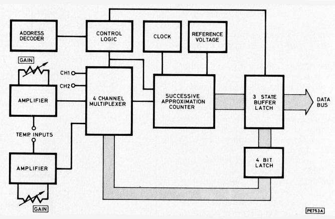
Two-channel temperature interface plus dual analogue ports for the Amstrad and the Spectrum This interface was designed to give the Amstrad CPC464 computer four analogue inputs, two of which are intended for use with semiconductor temperature sensors to give a measuring range of 0 to 51 degrees Centigrade with 0*2 degree resolution. However, the unit can be used as a straightforward four channel analogue to digital converter if desired. Although the unit was not designed with the Spectrum computer in mind, it has been tried with this computer and worked perfectly well. The only modification required for use with the Spectrum is the use of a different edge connector. The two analogue inputs have a full scale sensitivity of 1-2V and can be used together to provide a single differential input. If the inputs for the two temperature sensors are used as ordinary analogue inputs they have a full scale value which is adjustable from about 350mV to 1-2V. The sensitivity of each channel is individually adjustable. All four channels offer an accuracy of plus and minus 1 l.s.b. SYSTEM OPERATION A circuit of this type could be quite complex, but in this case things are kept remarkably simple by using a modern four-channel analogue to digital converter chip (the ADC0844CCN) and an equally modem temperature sensor chip (the LM35DZ). Fig. 1 shows the block diagram for the interface, and several of these blocks represent the internal circuit of the ADC0844CCN.
At the heart of the unit is the single successive approximation converter of the ADC0844CCN. The way in which this type of converter functions has been described in previous articles in this magazine, and we will not consider this aspect of the unit in detail here. While not providing ultra-fast conversions, the successive approximation technique is reasonably fast and can be achieved by a relatively low cost device. In the case of the ADC0844CCN the conversion time is no more than 40^s, and at 25 degrees Centigrade is typically 30ns. This enables up to about 25000 conversions per second to be achieved, which is more than adequate for the vast majority of applications. The reason for the exact conversion time being temperature dependent is that the ADC0844CCN has a built in clock oscillator which includes on chip timing components. The lack of frequency stability that this inevitably produces is of little practical importance, and it helps to minimise the number of discrete components that are needed. Unlike many analogue to digital converter chips, the ADC0844CCN does not include an internal reference voltage source. The full scale value of the converter is equal to the reference voltage used, and this can be any voltage of 5V or less. In the interest of good linearity it is not advisable to use a reference potential of much less than about IV though. In this circuit a highly stable 1-2V reference source is utilized. A four-channel analogue multiplexer ahead of the converter provides the unit with its four input channels. This is not as good as having four separate converters as each channel in use has to be read in turn. With all four channels in use this enables each channel to be read only about 6000 times or so per second, but even this reduced rate is far higher than is required for most applications. The required channel is selected by writing data to the converter, but only the four least significant bits are utilized when doing this. The data is stored in a four-bit latch, and in addition to selecting the channel to be converted it also sets the operating mode of the device and initiates a conversion. There are three operating modes, and these are single ended, differential, and pseudo differential. The single ended mode is the normal one where each input responds to the input voltage relative to the earth rail. In the differential mode the converter becomes a two-channel type with one pair of input voltages applied to channels 1 and 2, and the other two applied to channels 3 and 4. In the pseudo differential mode the unit is reduced to three channels (1, 2, and 3) with channel 4 being used as the inverting input for all three channels. This mode is not really applicable in this case due to the amplifiers added ahead of the channel 3 and channel 4 inputs. When a conversion has been completed the result is stored in an eight-bit data latch which has three state outputs. The outputs of the latch can therefore be connected direct to the data bus of the computer. Although the converter has four channels it only occupies one address, and the channel read at that address is the one previously selected by a write operation. Even if the same channel is read each time, a write operation must precede the taking of each reading in order to initiate fresh conversions. Otherwise the same conversion would be read repeatedly.
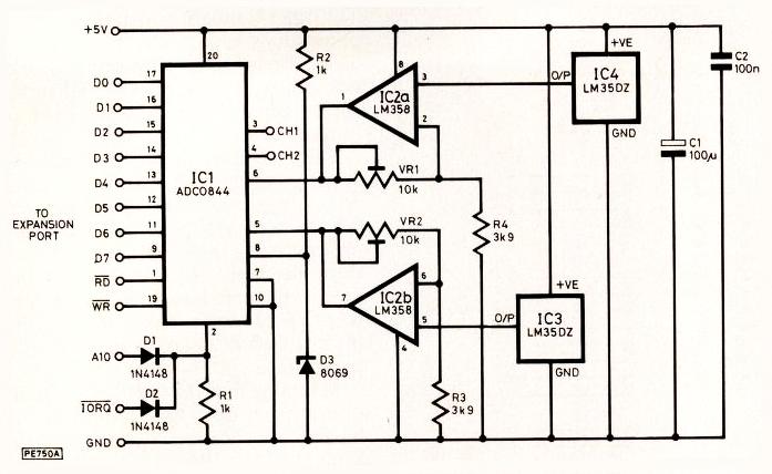
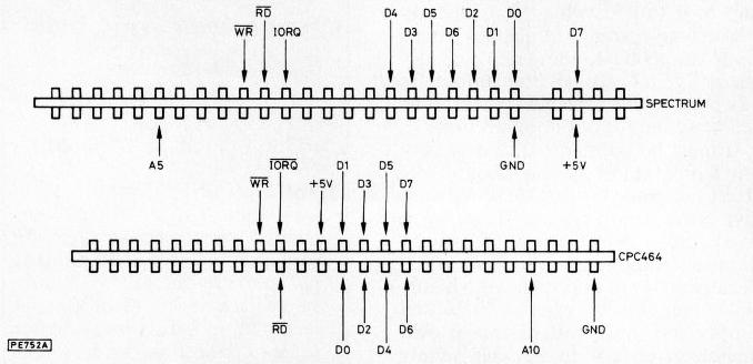
The address decoder is extremely simple, and only decodes one address line plus one control line. This is made possible by the simple system of input/output mapping used in the CPC464 and Spectrum computers, plus the fact that the ADC0844CCN is specifically intended to interface with 8080/Z80 based systems, and has inputs for the RD (read) and WR (write) lines. TEMPERATURE SENSOR There are normally difficulties if a semiconductor temperature sensor is connected direct to the input of an analogue to digital converter without using some form of signal conditioning circuit. For example, the popular LM335Z provides an output of 10mV per degree Kelvin, or 2-73V plus 10mV per degree Centigrade in other words. A temperature range of (say) 0 to 50 degrees Centigrade therefore gives an output voltage range of 2-73V to 3-23V. Obviously the output of the sensor could be fed to an analogue input having a full scale value of 3-23V, but this would be a very inefficient way of doing things since input voltages from 0V to 2-73V would never occur, and most of the converter's input range would be wasted. This is not merely of academic importance, and in practice would result in the system having relatively poor resolution and accuracy. Much better results could be obtained using a signal conditioning circuit to remove the 2-73V offset, and to spread out the 0 to 50 degree range over the full input voltage range of the converter. This type of manipulation is rendered unnecessary by the LM35DZ temperature sensors used in this design. These have a built-in circuit to eliminate the offset voltage, so that the output voltage is nominally lOmV per degree Centigrade. This gives a 0 to 510mV output voltage range over the 0 to 51 degrees Centigrade temperature span covered in this case. A simple d.c. amplifier at each of the two temperature sensor inputs boosts this to a 0 to 1-2V range which fully drives the converter. The converter provides readings of 0 to 255, which conveniently converts to readings in degrees Centigrade simply by dividing returned values by five. The gain of both amplifiers has been made variable so that they can be set up for optimum accuracy. It must be pointed out that at very low temperatures of only about 1 degree Centigrade the LM35DZ may not give good accuracy, but it will give good results over a range of 2 to 51 degrees Centigrade. In its favour it has the advantage of not requiring a highly stable supply, or even a stabilised supply for that matter, and it will operate over a 4 to 30 volt supply range. With a current consumption of only 56jiA there is little self heating. CIRCUIT OPERATION The full circuit diagram of the interface appears in Fig. 2. D3 and R2 form a shunt regulator which provides the 1-2V reference for converter chip IC1. D3 is not an ordinary Zener diode, but is a highly accurate and temperature compensated regulator chip. IC2 provides the two amplifiers which are conventional operational amplifier non-inverting mode types. The LM358 is one of the few operational amplifiers that is capable of providing output voltages right down to the earth rail, and this renders a negative supply rail unnecessary. IC3 and IC4 are the two LM35DZ temperature sensors. The unit connects to the floppy disc port of the CPC464 computer, which is really a general purpose expansion port having the full buses etc. available. The system of input/output mapping used in the CPC464 is to have circuits activated by taking one the eight most significant address lines low. One or more of the eight least significant address lines can be decoded as well if an input/output circuit requires several addresses (which is obviously not the case here). Address line A10 is available for external add-ons, and this line is decoded with the IORQ (input/output request) line and used to generate the negative chip select pulse for ICT. Dl, D2, and R1 form a simple 2-input OR gate. The interface is placed at address &F800 in the input/output map. Of course, as there is only partial address decoding the circuit can be activated using a large block of addresses, but the one mentioned above is the base address and is a convenient one to use in practice. In essence the system of input/output mapping adopted for the Spectrum is the same as that used in the CPC464. There is a slight difference in that one of the lower eight address lines is taken low to activate input/output circuits, and one or more of the upper eight address lines are used if additional addresses are required. For the Spectrum it is address line A5 that is gated with the IORQ line, and address 65503 that the circuit occupies. Again, due to the partial address decoding the circuit occupies a great many addresses, but in practice 65503 is probably the best one to use.
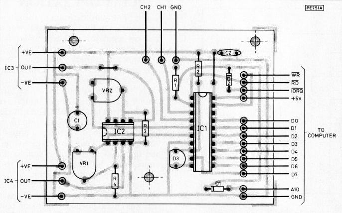
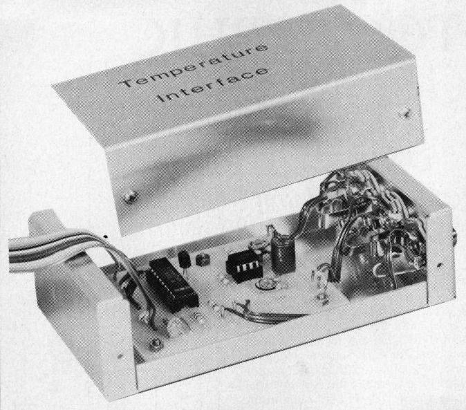
POWER SUPPLY The circuit requires a single (+5V) supply. The current consumption is only a few milliamps, and both the CPC464 and the Spectrum can readily supply this. CONSTRUCTION Fig. 3 shows the printed circuit board design for this interface. An important point to note is that IC1 is a CMOS device and should accordingly be fitted in a (20 pin d.i.l.) i.e. holder. The other standard antistatic handling precautions should also be observed. There are two link wires which should not be overlooked, but in other respects construction of the board is quite ordinary. The exact form that mechanical construction of the unit takes will depend on how it is to be used. It can simply be left as a loose board or, like the prototype, it can be built into a case. A third alternative is to incorporate the unit in to some larger piece of equipment. Whatever method is used the printed circuit design of Fig. 3 should be satisfactory.
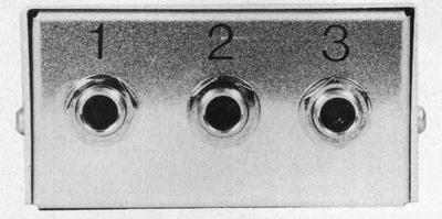
Assuming that the unit is to be built into its own case, an aluminium box having approximate outside dimensions of 133 by 70 by 38mm is suitable. The temperature sensors would not normally be mounted on the printed circuit board, but would be remotely located and connected to the interface by way of three-way cable. In order to minimise problems with stray pick up of noise it is advisable to use twin overall screened cable, with the screen carrying the negative supply rail connection. On the prototype three stereo jack sockets are mounted on the front panel, and connections from the sensors to the printed circuit board are made via two of these. The third one is used for the two ordinary analogue inputs.
A 14-way ribbon cable up to about one metre long connects the printed circuit board to the floppy disc port of the CPC464 or the expansion port of the Spectrum. For the Amstrad computer a 2 by 25-way 0-1 inch pitch edge connector is required. As it is unlikely that a connector having a suitable polarising key will be available care must be taken to fit the connector the right way up, and it is advisable to clearly mark the top edge. The Spectrum's expansion port requires a 2 by 28-way Ol inch pitch edge connector, and types having a suitable polarising key are readily available. Fig. 4 gives connection details for both computers. Take great care not to make any wiring errors, and thoroughly check all the wiring once it has been completed. With the specified case it is possible to take the ribbon cable out between the top and base sections, but if an alternative is used it might be necessary to cut an exit slot in the rear panel.
TESTING AND USE Start with VR1 and VR2 set at about half maximum resistance. Connect the interface to the computer before switching on the computer. The two simple programs shown in Table 1 can be used to give a temperature readout From BASIC, the OUT instruction is used to write the appropriate number to the converter to start a conversion and select the required channel. The number is 6 to read IC4 and 7 to read IC3. The INP function (IN for the Spectrum) is used to read the converter, and as explained earlier, dividing the reading by five gives a reading in degrees Centigrade. The relative slowness of BASIC means that a conversion will always have been completed by the time the unit is read, but when using machine code a delay loop to provide a hold off of at least 40µs will be required. In order to calibrate the unit both sensors should be taken to a known temperature, and one that represents about 50% to 100% of the full scale value. The two presets are then adjusted to give the correct reading. If the sensors are to be used in liquids they should be fitted in a small test tube or a similar container to protect them. Some silicon grease can be used to give a good thermal contact between each sensor and its container. In the single ended mode analogue channels 1 and 2 are selected using values of 4 and 5 respectively. When these are used as a single differential input they are selected using values of 0 (channel 2 is the inverting input) or 1 (channel 1 is the inverting input).
|


