


★ HARDWARE ★ MONTAGES ★ AMSTRAD SPEECH SYNTHESIZER (EVERYDAY ELECTRONICS) ★ |
| Amstrad Speech Synthesizer (Everyday Electronics) | Hardware Montages |
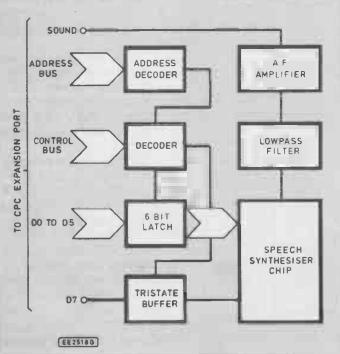
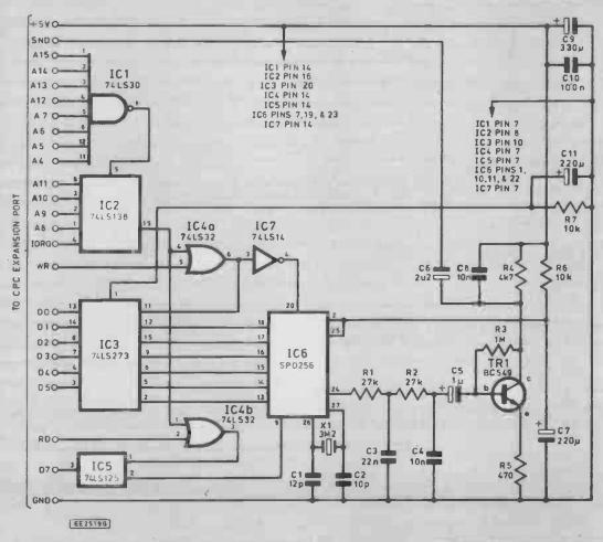
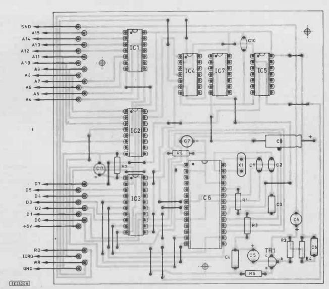
Low-cost voicing for your Amstrad. Based on the popular SP025G "speech" chip. Although they rank as one of the most popular computer ranges, the number of published add-on projects for the Amstrad CPCs seems to be relatively small. Possibly this is due to the fact that Amstrad launched these computers after the main home computer boom, when interest in computer projects had waned somewhat. Anyway, this article describes an add-on speech synthesiser for any computer in the CPC range, and helps to rectify the lack of projects for these machines. The unit fits onto the CPC expansion port, and provides its speech output via the computer's built-in loudspeaker. The circuit is based on the popular SP0256 speech synthesiser chip This is a relatively cheap speech chip, but is one which gives an unlimited vocabulary. Fig. 1. The Amstrad CPC Speech Synthesiser block diagram. >> Unlike some methods of speech synthesis, the one used by the SP0256 does not require large amounts of the computer's memory in order to store a few words. In fact a dozen long sentences would probably require no more than about IK of memory. The speech quality is not as good as some systems, but is quite acceptable. Considering uie simplicity of the system used in this method of speech synthesis, the speech quality is remarkably good. ALLOPHONES There is a slight drawback in using the SP0256 speech chip, and this is simply that it is relatively difficult to program well. It produces words by stringing together a number of “allophones”, w ch are the basic sounds of speech. For example, “shhhh”, “arrr”, and “ow” are the sort of simple sounds that can be fitted together to make up the more complex sounds of complete words. These words, separated by pauses where necessary, can then be put together to make complete sentences, or even a number of sentences if required. For this system to be successful you must have at your disposal all the sounds needed to make up all the words in the language. Apparently the sounds required vary significantly fiom one language to another, ind the sounds for a particular language are called “phonemes”. The SP0256 contains sixty four phonemes (including pauses) that permit any English word to be produced. For this system to work well the allophones need to be chosen very carefully, and the obvious ones are not necessarily the ones that give the best results. How-ever, with a little experience it is possible to put together some intelligible sentences in a reasonably short space of time, perhaps with a little “fine tuning” being needed in order to get things just right. SYSTEM OPERATION The block diagram of Fig.l shows the basic arrangement used in this speech synthesiser. The speech synthesiser chip is at the heart of the unit, and th.s includes a 2K by 8 ROM that contains all the allophones. It has provision for operation with up to three external ROMs, giving a maximum capacity of 256 allophones. However, in most circuits (including this one) no external ROMs are used. There are 64 allophones available to the user, and these are selected via six address inputs. Rather than a true audio output, the SP0256 provides a pulse width modulated output signal. In other words, the output signal is a high frequency pulse signal, with the pulse width being varied to give the required audio output voltage. A high mark-space ratio gives a high average output voltage, a low mark-space ratio gives a low average output potential, and a 1 to 1 ratio gives an intermediate average output level. By varying the pulse width the average output voltage can therefore be made equal to the required audio output potential. In order to decode this type of signal it is merely necessary to pass it through a lowpass filter. This filters out the pulses a.id leaves a potential equal to the average voltage of the pulse signal. The output signal from the lowpass filter is too low to drive the audio input of the CPC computers properly, and so the signal is boosted by an amplifier before being fed to the computer. INTERFACING Interfacing the SP0256 to the buses of a computer is reasonably straightforward. In order to produce a series of allophones from the chip it must first be fed with a 6-bit allophone address. Then, in order to get the chip to produce the selected allophone, a pulse must be applied to the chip's “ALD” (allophone load) input. It is important that the next allophone is not sent to the SP0256 until it has completed the current one. Otherwise, each allophone, apart from the final one, is cut short to make way for the subsequent one, giving what is just a brief burst of noise from the loudspeaker. The SP0256 provides a sort of “handshake” output in the form of its “LRQ” (load request) output. This is normally low, but it goes high when the chip is producing an allophone. The flow of data can be correctly controlled by using a software routine to send an allophone address to the SP0256, wait until “LRQ” goes low, send another allophone address, monitor “LRQ” again, and so on, until all the allophones have been produced. Timing loops are not really a viable alternative as the allophones have various durations from 10ms to 420ms. An accurately timed flow of data is essential if a good quality output is to be achieved. In my experience at any rate, feeding the address inputs of the SP0256 direct from one of the computer's buses is not likely to be successful. More reliable results are usually obtained if it is fed from a latching output port. In this case it is driven from a 6-bit latching output derived from data lines D0 to D5. The “ALD” input of the speech chip is driven from the “write” output of the address/control bus decoder circuit. Consequently, writing an allophone address to the SP0256 results in that allophone being automatically produced by the device. Fig. 2. Complete circuit diagram for the Amstrad CPC Speech Synthesiser. >> The “LRQ” output of the SP0256 is fed to D7 of the data bus via a tristate buffer. Note that data line D6 is not required by the speech synthesiser, and that this line of the computer's expansion port is left unconnected. DECODING With an unexpanded CPC464 it is possible to utilize a very simple form of address and control bus decoding, which more or less consists of activating the interface when A10, IORQ, and either RD or WR are all low. With expanded or disk based CPCs the situation is a little more tricky, and much more precise decoding is required if interactions between the user add-on and other hardware (particularly the disk drivers) are to be avoided. In this circuit all the address lines from A4 to A15 are decoded so that the speech synthesiser is placed in the input/output map at address &F8F0. In fact is appears at “echoes” from &F8F0 to &F8FF, and can be accessed by way of any address in this range. The address/control bus decoder provides separate “read” and “write” outputs. Address &F8F0 is therefore used for sending allophone addresses to the SP0256, and for monitoring its “LRQ” output. CIRCUIT OPERATION Refer to Fig.2 for the full circuit diagram of the Amstrad CPC Speech Synthesiser. IC6 is the SP0256 speech chip, and this has a built-in clock oscillator. It requires a discrete crystal and two capacitors (XI, Cl, and C2), and the clock frequency recommended by the speech chip manufacturer is 3.12MHz. << Fig. 3. (above) Printed circuit board component layout and wiring details, (below) Full size printed circuit copper foil master pattern. >> The second complication is that we require separate outputs for read and write operations. This is achieved by gating the output of IC2 with the RD (read) and WR (write) lines of the CPC expansion bus, using a separate OR gate for each of these two lines. This gives a negative read pulse from IC4b, and a negative write pulse from IC4a. A positive pulse is needed for the ALD input of the speech chip, and this is derived from the write output via inverter IC7. The six bit latching output for IC6 is provided by IC3, which is actually an octal D type flip/flop. In this case only six of the flip/flops are used, with the two “spares” just being ignored. IC4a provides a negative pulse to the “clock pulse'' input of IC3 during write operations to the interface, and this latches the outputs of the flip/flops. At switch -on a negative reset pulse is supplied to IC3 by C11. This ensures that IC3 commences with all its outputs low, and that the speech chip does not produce any output until the user activates it. R7 ensures that C11 is rapidly discharged when the computer is switched off, so that a fresh reset pulse is produced when it is switched on again. ICS is a quad tri-state buffer, but in this circuit only one buffer is used and no connections are made to the other three. It interfaces the LRQ output of IC6 to D7 of the CPC expansion bus, and it is set to the active state by the output pulses from IC4b during read operations to the speech synthesiser. Power for the speech synthesiser is obtained from the +5 volt supply output of the CPC expansion port C9 provides smoothing which helps to give a low noise level on the audio output of the unit.
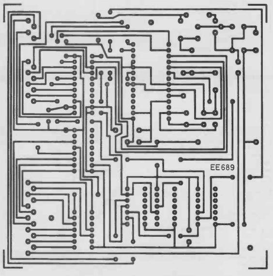
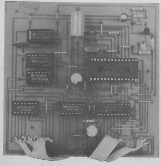
CONSTRUCTION Details of the printed circuit board are provided in Fig.3. Crystal XI must be a miniature wire-ended type with 0.2 inch lead spacing if it is to fit easily onto the board. Try to complete the soldered joints reasonably rapidy when fitting this component as some crystals are relatively easily damaged by heat. IC6 is a MOS integrated circuit, and as such it is vulnerable to lamage by static charges.
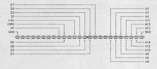
Leave this component in its anti-static packaging until, in all other respects, the unit is finished. Then fit this component onto the board, handling it as little as possible, avoiding touching the pins and fitting it into a holder already fitted to the board so that there is no need to make any direct soldered connections to this chip. With a fairly large integrated circuit of this type, IC6 can be a bit difficult to fit a into its socket. Usually the pins have to be carefully bent inwards slightly. Be careful not to buckle any of its pins when fitting IC6 into its socket. Although none of the other integrated circuits are static sensitive types, it is recommended that they should be fitted in holders. Fig. 4. Connection details for the 2x25 way edge connector. >> There should be no difficulties in fitting the other components onto the board provided the correct types of capacitor are used. In particular, the polyester types should have a lead spacing of 7.5 millimetres (0.3 inches). Be careful to fit the electrolytic capacitors with the correct polarity. A number of link wires are required, and these can be made from 22s.w.g. tinned copper wire, or the leads trimmed from the resistors and capacitors might be sufficient. CONNECTIONS The board is connected to the computer via a 25-way ribbon cable which is fitted with a 2 by 25-way 0.1 inch pitch edge connector at the computer end. At the other end it is either connected directly to the board, or via pins if preferred. Both ends of the cable should be prepared by separating all the wires, stripping a few millimetres of insulation from each one, and tinning them all with solder. The terminals of the edge connector (or the twenty five that are used anyway) should be tinned with solder, as should the pins on the board if this method of connection is adopted. In my experience the CPC computers are not tolerant of long connecting leads on their expansion bus. It is therefore recommended that the connecting cable should be no more than about 0.6 metres long. The edge connector connection details are given in Fig.4. The board has been designed so that the order of the connections on the board matches up well with that of those on the edge connector. Therc-is no need for any crossing over of wires, but you still need to be very careful to get each lead connected to the right terminal of the edge connector. The multi-coloured “rainbow” ribbon cable is better for this sort of thing, but grey ribbon cable is usable if you take extra care. If you are using a connector fitted with the appropriate polarising key, make quite sure that you have the connector the right way up before making the connections to it If the connector is not fitted with a polarising key, clearly mark the top and bottom edges such as to minimise the risk of fitting it to the expansion port up-side-down. Once this wiring has been completed, check it very thoroughly at least once before connecting the unit to the computer and trying it out. Projects of this type are often left as incased boards, as was the prototype. However, it should not be difficult to fit the unit into a small plastic case if preferred. This does have the advantages of being a bit neater, and keeping dust etc. off the circuit board.
|


